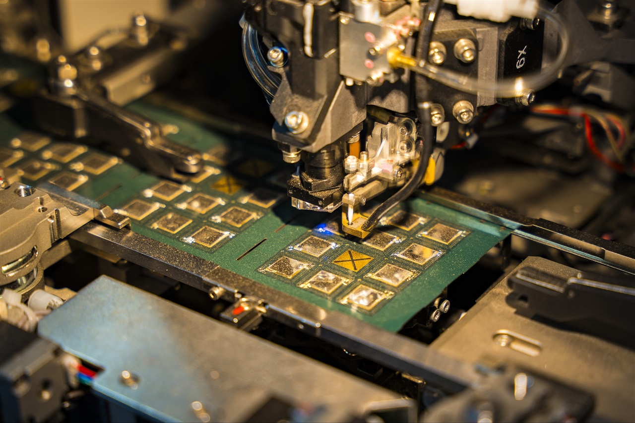
On March 24, 2025, Jiufengshan Laboratory (JFS) announced two major breakthroughs in GaN technology: the world’s first 8-inch silicon-based N-polar gallium nitride on insulator (GaNOI) material with high electron mobility, and the debut of China’s first 100nm GaN process design kit (PDK) for chip fabrication.


